 English
 Español
 Русский
 Français
 Deutsch
 Português
 Italiano
Products
The new crystal was developed to be applied in blue LED components, InGaN blue-violet semiconductor lasers and other light emitting components that use GaN substrates. Compared to most sapphire substrates used in LED components, SCAM is more compatible in lowering flaws in GaN semiconductor crystals, which could improve the lighting component’s luminosity. A feature of SCAM crystals is GaN lattice mismatch is down to only 1.8 percent, crystals are less likely to have this flaw. Industry insiders used to believe it is extremely difficult to make SCAM crystals, but the laboratory has successfully made the crystals using Czochralski method crystal growth.
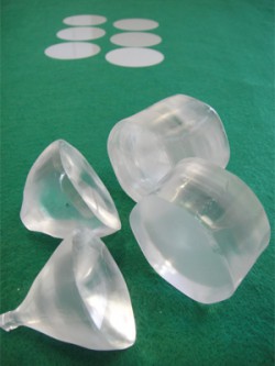
Fukuda Crystal Laboratory has sucessfully synthesized SCAM crystal for blue LED applications.
By improving crystal growth environment and the crystal growth furnace, the laboratory was able to improve the quality of the crystals. The laboratory used X-ray scattering techniques to assess the c-plane of the SCAM crystal, and found its half-amplitude duration was 12.9 seconds, indicating the crystal quality was the same as silicon crystals.
Additionally, the laboratory abandoned cutting and polishing technology. Instead they sliced open SCAM caking of crystals and with some processing them into wafers. This greatly reduced wafer costs. Using MOCVD technology, under 1040 degrees Celsius the laboratory enabled GaN films to grow vertically on the sliced side of the SCAM crystal to create a mirrored low dislocation crystal.
According to the laboratory, the research team headed by Professor Matsuoka Takashi from the Institute for Materials Research at Tohoku University used products from test trials to design a layered GaN semiconductor LED, and has proven the material is effective.
The Fukuda Crystal Laboratory will continue to work on broadening SCAM crystal width and commercialization of the crystal. The laboratory plans to sell the 2-inch SCAM substrate by spring 2015.